Inspecting PWM3320DB-TYDU SPI with Logic Analyzer
In my previous post I failed to get an Arduino working as a logic analyzer to inspect the SPI communication between the EX-G trackball controller and the PWM3320DB-TYDU optical sensor. I ended up ordering a Lonely Binary logic analyzer in the hopes that it would be able to capture the SPI communication.
I’m going to spoil the results and say that the logic analyzer worked wonderfully! I’m also going to skip over the 30 minutes to an hour I spent figuring out how to work with the Saleae Logic Pro 2 software and the logic analyzer. I will jump right into the final setup that I ended up with.
Connecting the Logic Analyzer
The logic analyzer kit comes with 10 test clips. 5 mini grabber hooks, the round ones. 5 IC test hooks, the rectangular ones. The kit also includes 5 alligator clips and a ribbon cable for connecting breadboard header pins.
Looking at the test clips there is no immediate way to connect either the alligator clips or the breadboard header pins to them. As an example, these IC test hooks on Amazon include a place to connect jumper leads.
After scratching my head for a bit, I realized one can pull off the back part off of the IC test clips.
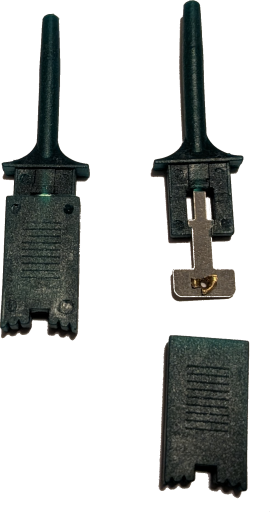
Longer term I would like to feed a wire through the back and solder it to the hole in the exposed tang. For now I can get by attaching the alligator clips to the exposed tang.
The test clips are called “IC test clips” because they work well for connecting to ICs. So I will use them to connect directly to the PWM3320DB-TYDU IC, instead of trying to use the touch points on the EX-G printed circuit board.
The data sheet for the PWM3320DB-TYDU shows the circle indentions that are present on the physical IC. This allows one to more easily identify which pins are which.
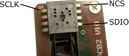
I attached:
GNDof the logic analyzer to the battery ground wire of the EX-G, using the black alligator clip.- Pin 2 of the logic analyzer to the
SDIOleg of the IC, using the red test clip and red alligator clip. - Pin 4 of the logic analyzer to the
SCLKleg of the IC, using the yellow test clip and yellow alligator clip. - Pin 5 of the logic analyzer to the
NCSleg of the IC, using the green test clip and green alligator clip.
The colors to pin mappings were chosen to match the channel colors and order in the Logic Pro 2 UI.
One thing to note is that the order of the terminals on the logic analyzer board for the alligator clips is not sequential. They are 0, 2, 4, 6, 1, 3, 5, 7.
Configuring Logic Pro 2
The Lonely Binary website has some brief instructions on installing and using Logic Pro 2, https://lonelybinary.com/en-us/blogs/logic-analyzer-quickstart-1/03-logic-2.
Summarizing:
- Download the software from Saleae
- Install the software that was downloaded
- Connect the logic analyzer to the computer
- Launch the installed Logic Pro 2
By connecting the logic analyzer first, Logic Pro2 will automatically identify the analyzer and get right to the start screen.
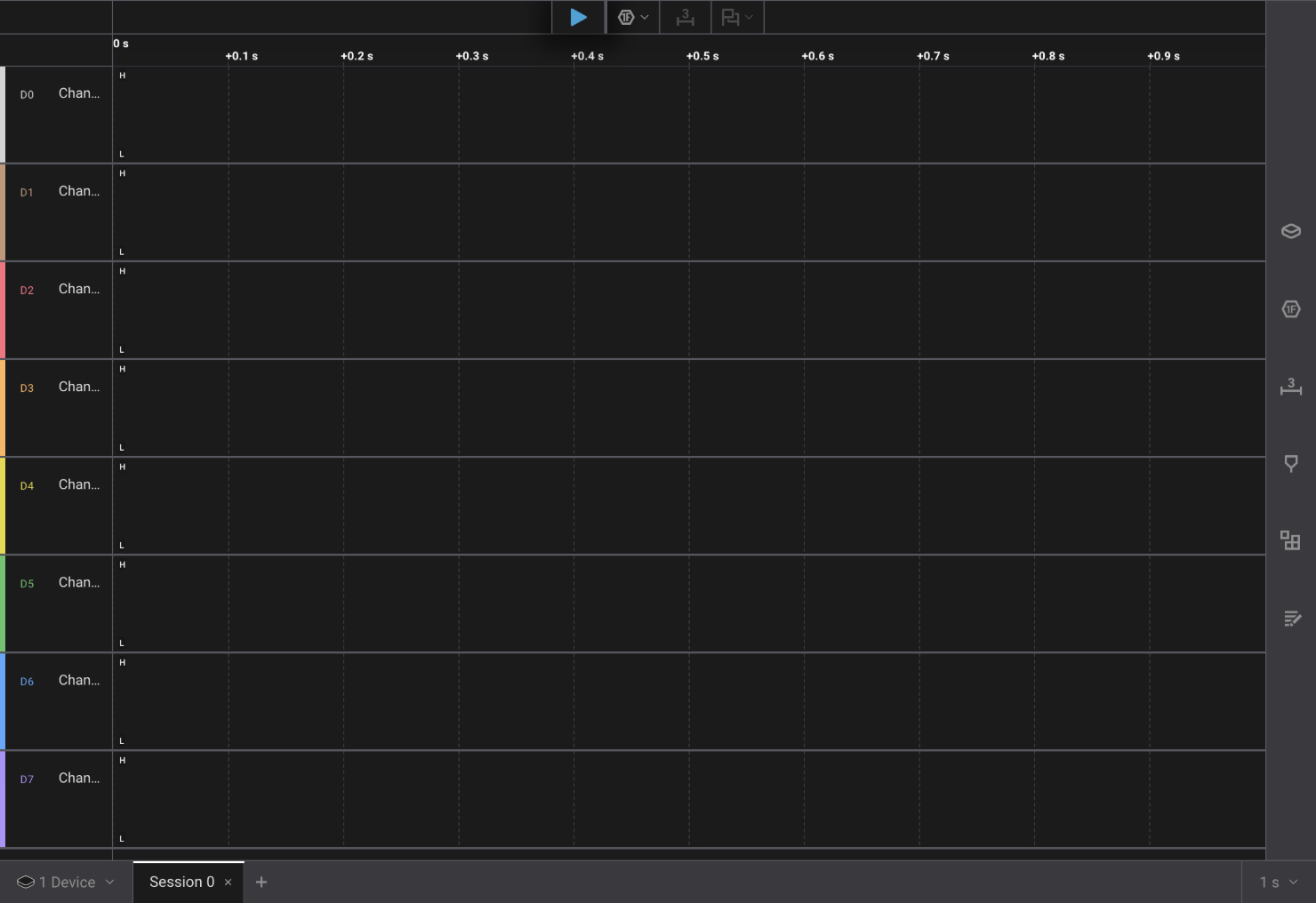
The start screen will be more or less empty, showing all the possible channels.
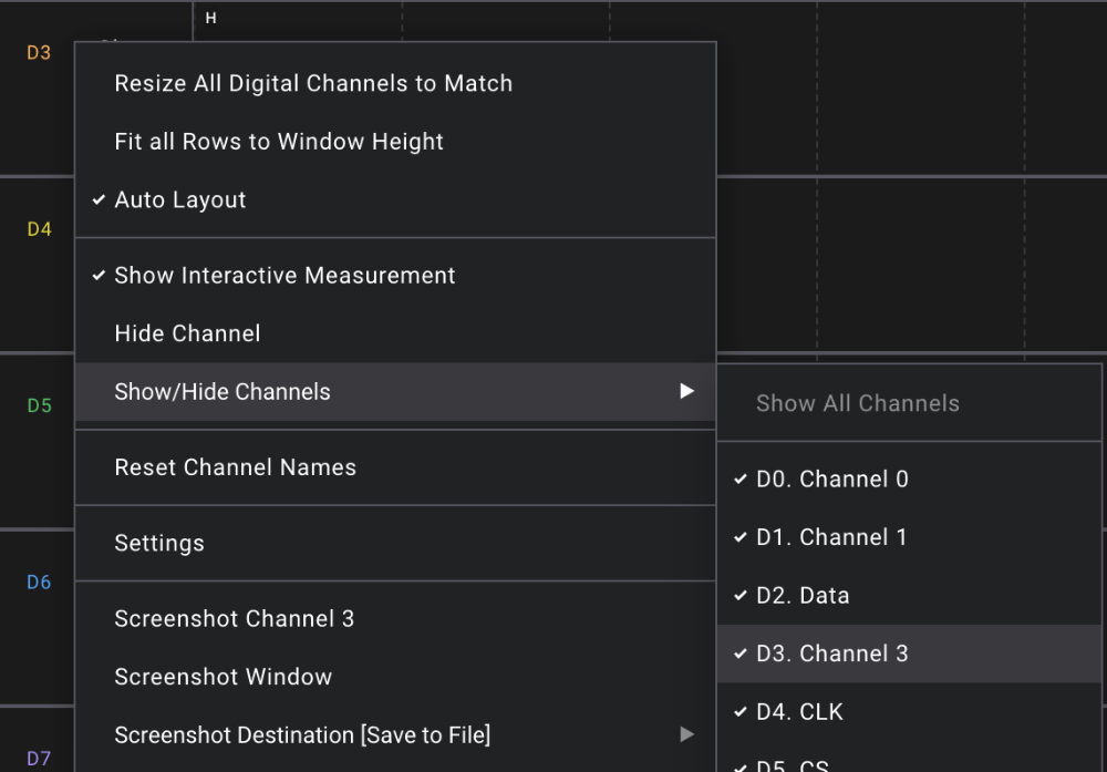
The first thing I did was rename the channels that I was using. This is done by
selecting the “Chan…” text at the very left of the channels. I named D2
Data, D4 ClK, and D5 NCS.
After the channels were renamed, I hid the other channels I wasn’t using. The dialog to hide channels is opened by right clicking in the area where the channels were renamed. The channels are hidden by unchecking them in the dialog.
The next thing I did was add trigger settings. Trigger settings allows the logic analyzer to be looking at the data, but to not actually record until the trigger happens. To get to trigger settings, click on the “Device Settings” button on the right of the Logic Pro 2 window.
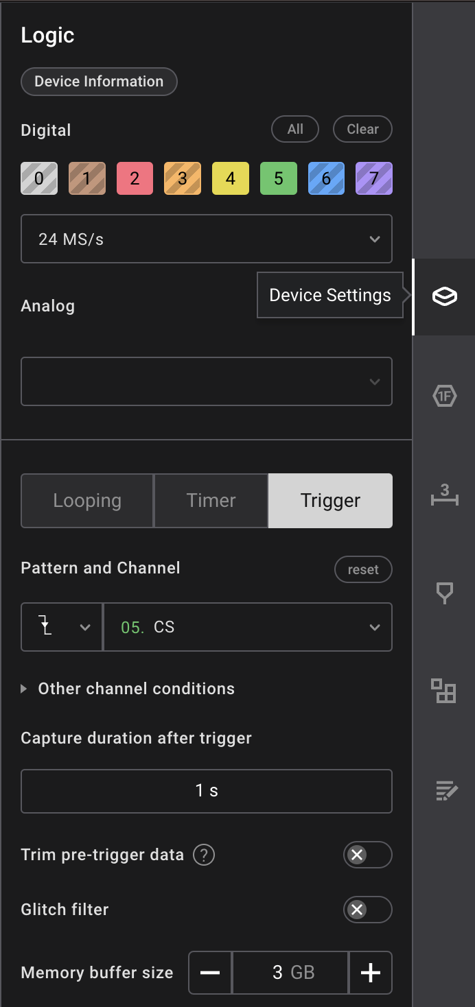
- Choose sampling rate of
24MS/s - Choose the
Triggerbutton - Choose “Falling Edge” for pattern
- Choose channel 5
CS
I chose CS as that has to be held active while instructions are being sent on
the SPI. The “Falling Edge” pattern is because the CS is normally high and
goes low when active. This trigger will happen when CS goes low, or active.
Next I configured the Logic Pro 2 to decode the data as SPI. This is done by selecting the “Add Analyzer” at the top of the window and searching for SPI.
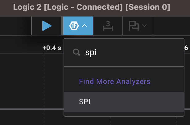
Selecting SPI from the dialog will open up an SPI settings dialog
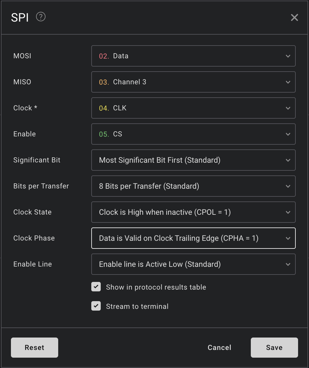
- Choose channel 2
Datafor “MOSI” - Choose channel 3 for “MISO”
- Choose channel 4
CLKfor “Clock” - Choose channel 5
CSfor “Enable” - Choose “Most Significant Bit First” for “Significant Bit”
- Choose “8 bits” for “Bits per Transfer”
- Choose “CPOL = 1” for “Clock State”
- Choose “CPHA = 1” for “Clock Phase”
- Choose “Enable line is Active Low” for “Enable Line”
The MISO channel doesn’t matter, but the dialog wants a channel for it.
Click save on the dialog and we’re ready to start capturing!
Capturing SPI data
I put a battery in the terminals of the EX-G board to power it on. I had the
wireless receiver hooked up to my computer and moved the track ball around to
ensure it was sending mouse move events to my computer. After I ensured it was
working I waited a couple of seconds to ensure no data was being sent to the
sensor. In the Logic Pro 2 software, I pressed the r key to start capturing.
Ensuring I didn’t bump the trackball, I moved the switch that controls DPI from
the 750 DPI position to the 1500 DPI position. Logic Pro 2 stopped streaming and
showed me the following screen.
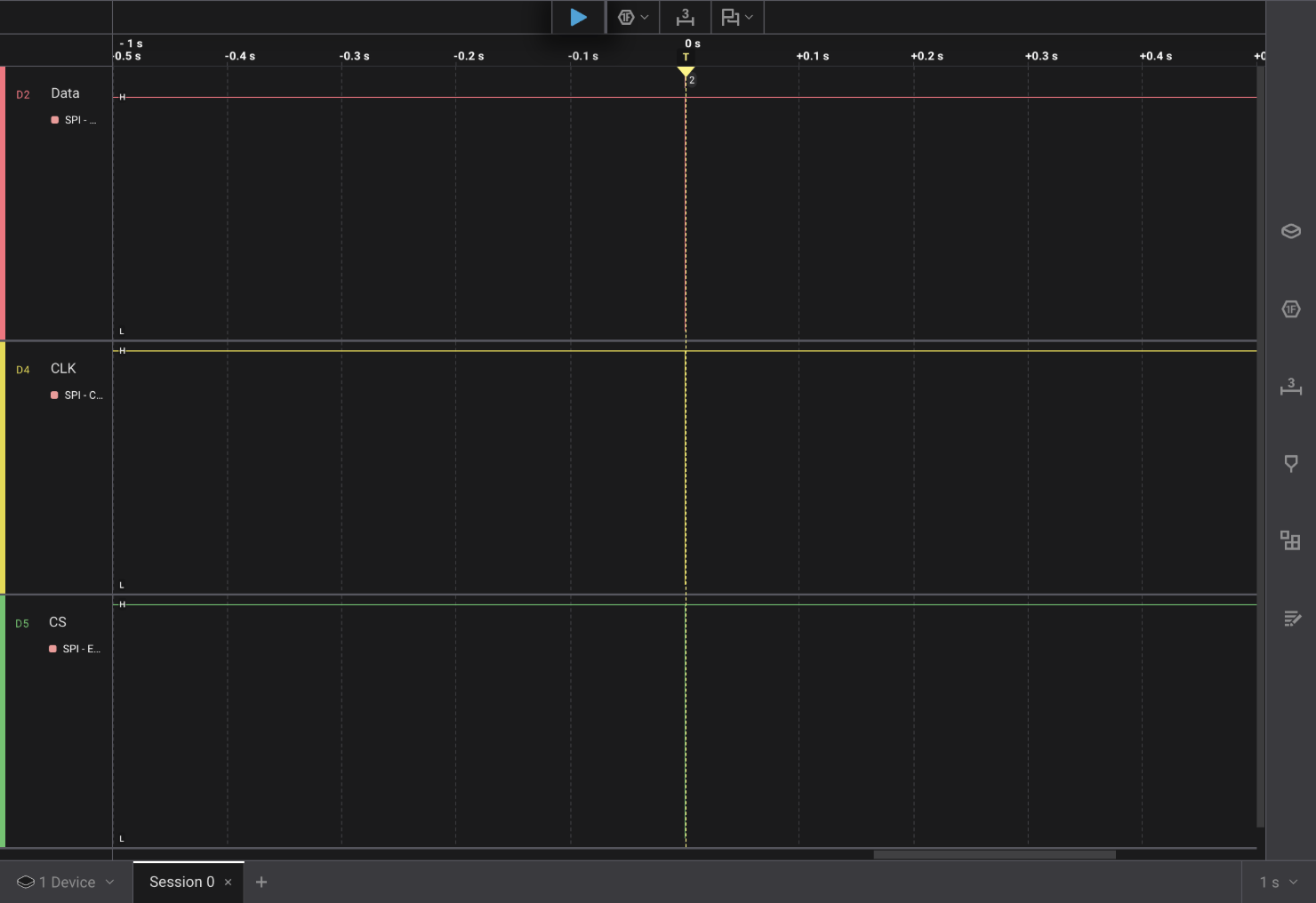
It doesn’t look like much, but hitting the = key a number of times I was able to zoom in and see the following:
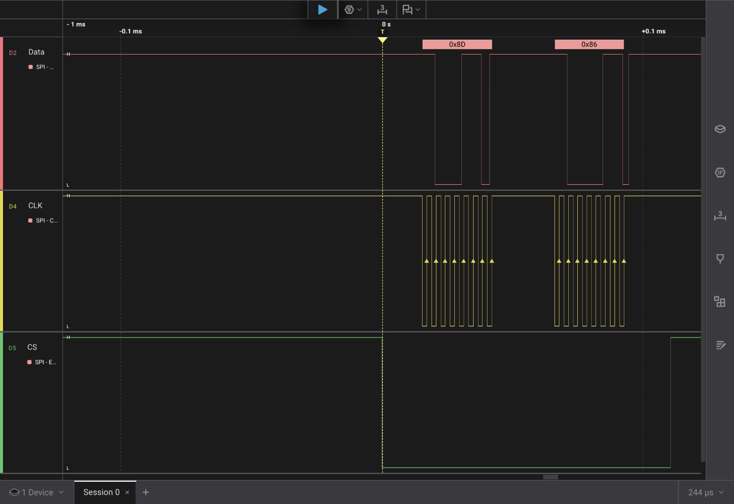
It’s a nice capture showing two bytes of data sent to the sensor, 0x8D and 0x86.
Looking back at
the SPI specification for
the PWM3320DB-TYDU, the 0x8D looks like it’s a write to register 0x0D.
Register 0x0D in the
data sheet
is the RESOLUTION register. This seems like the correct command we would
expect when changing the DPI. A write to the RESOLUTION register with a new
value.
I went ahead and restarted the capture with the same trigger. Then I flipped the
switch back to the low DPI setting. This captured two bytes that were 0x8D and
0x83. The data sheet for the PWM3320DB-TYDU mentions that it has 250 cpi/step.
0x86 - 0x83 is 0x03, or \(3\) in decimal.
cpiis the more correct unit, but marketing material often usesDPI. Hence why the EX-G saysDPI, while the PWM3320DB-TYDU data sheet usescpi.
The difference between the two values, 0x83 and 0x86 seems to correspond to
the available resolution. The most significant bit of the value being set may
seem odd, but looking at the
ADNS-3050 data sheet
it uses some of the other bits of the RESOLUTION for other purposes.
Clock Timing
I was a little surprised looking at the clock timing. This is probably due to my
lack of experience working directly with these kind of protocols. I was thinking
that
time keeps on ticking slipping
and that the clock would always be present and always be constant.
Looking at the capture we can see that CS is activated and then a bit later,
the CLK starts cycling. This implies to me that the CLK isn’t so much a
periodic signal as a only a synchronization signal. Where going active is a
signal saying to put the data bit on the Data line.
The clock also stops ticking between the write command byte and the data byte. In the ADNS-3050 data sheet it mentions a time between write commands (\(t_{sww}\)) with a value of 30 μs. Based on the 0.1 ms bar after the bytes, the gap looks to be pretty close to the30 μs wait time. My understanding of the wait time is it’s between commands themselves and not between the command and the commands data, but the EX-G may always wait that long for any byte that is part of a write command.
In hindsight, it makes sense that the clock is really just a synchronization event and it doesn’t need to strictly follow a consistent period. If it was set up to follow a consistent period then there would be less tolerance for delays. Handling the wait time between write commands could get tricky when close to a clock edge, likely requiring some kind of data prefix to indicate the start of a message. Only sending the clock during bit transfers also means less power used since the controller only needs to send the clock signal when talking to the PWM3320DB-TYDU instead of all the time.
Data Bit Values
I chose the “Most Significant Bit First” for decoding the SPI data as it was the
default. Ox8D is binary 0b10001101 and 0x86 is binary 0b10000110. The
bit value is sampled on the rising edge of the CLK. I would have thought that
the Data idle value would be treated as 0 and the active value would be
treated as 1. However based on the captures it seems that high is 1 and low
is 0.