Recording the traffic in the EX-G to PMW3320DB-TYDU
In the previous post, I was able to successfully snoop on the SPI traffic between the EX-G controller and the PMW3320DB-TYDU optical sensor.
The intent of this post is to capture all of the necessary communication between the EX-G controller and the PMW3320DB-TYDU in order to recreate the initialization of the PMW3320DB-TYDU as well as correctly read the sensors X and Y delta information to correctly move the mouse cursor on a computer.
Looking back at my initial investigation into Serial Peripheral Interface on PMW3320DB-TYDU, I had listed wanting to look at the SPI communication between the EX-G controller and the PMW3320DB-TYDU under the following conditions:
- power on
- reading track ball movements
- switch between 750DPI and 1500DPI modes
- switch between low power and high speed modes
My plan is to use the same setup for the logic analyzer as the last post and try to capture these scenarios.
Saleae logic pro 2 keeps your settings from last time. So using the same connection can save some setup work.
Power Up
The EX-G powers up by going from off to the low power mode. I’m going to use a
falling edge trigger on the CS channel, with the default duration of one
second. I hope that the PMW3320DB-TYDU is fully initialized within one second.
If I still see what looks like communication towards the end of the one second,
then I will increase the capture time.
With the power switch in the off position, I connected the battery. With the Saleae Logic Pro 2 recording, I turned the EX-G power switch to the low power position.
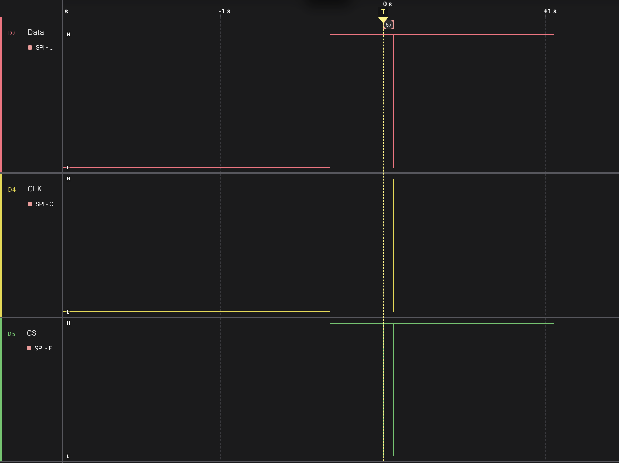
Looking at the above image, all the channels were low until about 1/3 of a second before the vertical dashed yellow line. The dashed yellow line is the trigger event that started the capture. It looks like it took that 1/3 of a second for the EX-G to power on enough to begin talking to the PMW3320DB-TYDU.
We can also see there was some initial communication that happened fairly close to the trigger event, and then there was nothing more for the rest of the one second capture. I think it’s safe to say the startup logic all happens in this short time frame.
Zooming in closer to the trigger event and follow on communication.
It looks like the power on traffic stops ~65ms after the trigger event occurred.
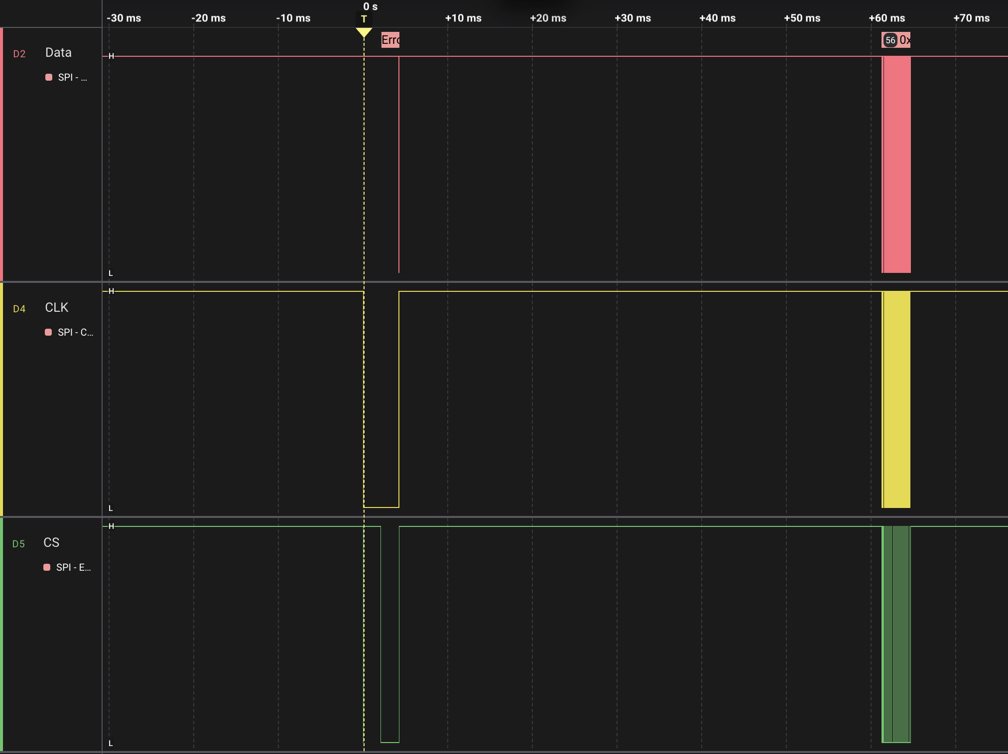
The start of the capture happens when CS first goes low. CS is the green
channel at the bottom of the image. It:
- goes low for ~10µs, this can be hard to see at this zoom since it’s so small.
- goes high for ~2ms
- goes low for ~2ms
- goes high for ~57ms
- bounces around after 60ms when it looks like
CLKandDATAare also bouncing around.
When the trigger event happens CLK:
- goes low for ~4ms
- goes high for ~57 ms
- bounces around after 60ms
DATA mostly stays high until the 60ms bouncing that all three channels do.
There is a slight drop low around the time that CS and CLK both go high for
~57ms.
Zooming into this dip we get the following:
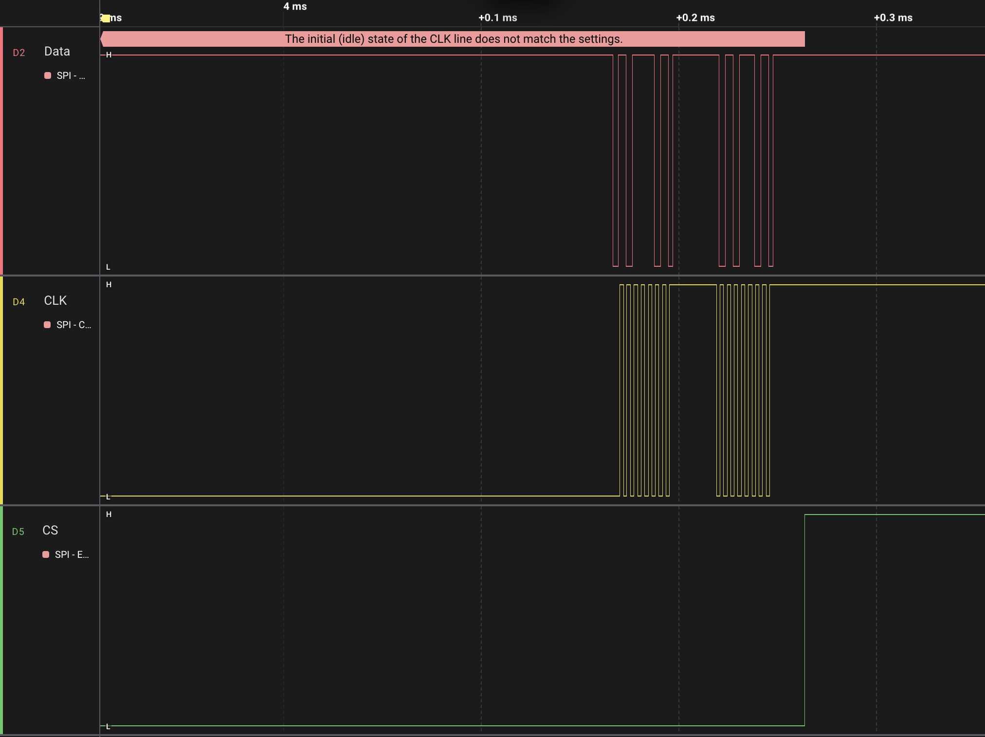
It looks like it might be an SPI message. We can see that logic pro 2 failed to
decode, due to the CLK line starting at a low value instead of the idle value
of high. Recall from the previous post that we were interpreting the data as
clock phase 1 (CPHA1). This means we read the data bit values when the clock
goes from low to high, because high is the idle value.
Manually reading these values I get 0b10111010, 0b01011010 or 0xBA, 0x5A.
Since the most significant bit of the first byte is 1 it’s a write command. If
we remove the MSB, it’s a write command to register 0x3A with a value of 0x5A.
Looking at the
data sheet,
0x3A is the POWER_UP_RESET register.
Looking at the
ADNS-3050
data sheet, it has a Power Up Reset section that says.
- Apply power
- Drive NCS high, then low to reset the SPI port
- Write 0x5a to register 0x3a
- Wait for at least tWAKEUP when performing reset from power down.
- Write 0x20 to register 0x0d
- Write 0x00 to register 0x41
- Configure the sensor
Looking elsewhere in the ADNS-3050 data sheet
tWAKEUPis 50-55ms.
It seems the first 60ms of the capture are steps 1-4 of the above.
- Power is likely applied when the lines go high
CSgoes low for 10µs temporarily in order to be driven high for 2ms, and then low for 2ms, resetting the SPI port- 0x5A is written to 0x3A
- Everything is idle for tWAKEUP, 57ms
Moving over to the bouncing after the tWAKEUP delay. We can see that these
are SPI messages:
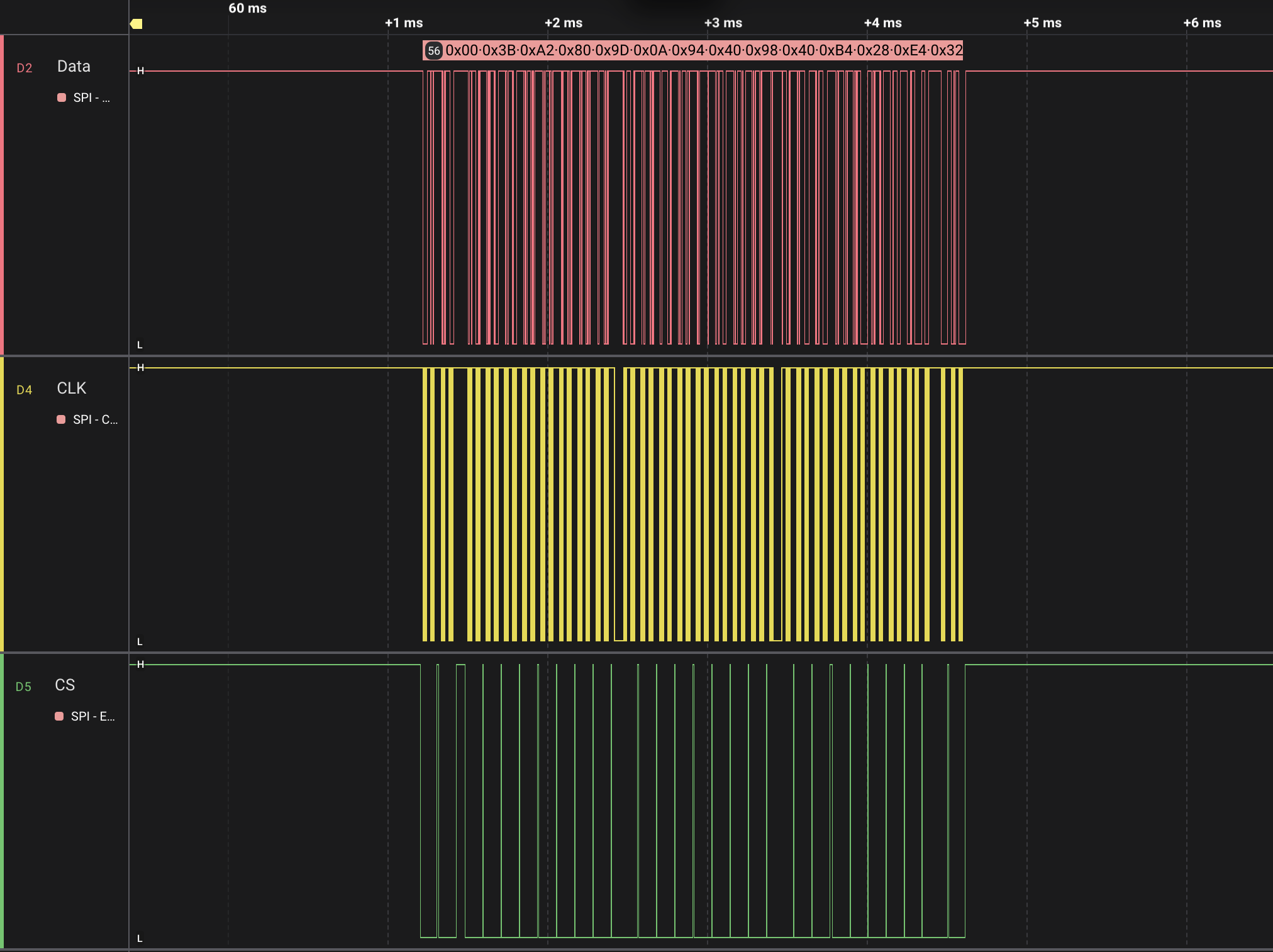
Notice in the image above that CS is going low and high multiple times while
all of the messages are being sent. The ADNS-3050 data sheet mentions:
To improve communication reliability, all serial transactions should be framed by NCS.
I’m guessing this is what they mean. Drive NCS high at the end of each read or write command. Drive it low before the start of the next read or write command.
The values decoded by Logic Pro 2 are:
| Command | Register | Value |
|---|---|---|
| Read | 0x00 PROD_ID | 0x3B |
| Write | 0x22 PERFORMANCE | 0x80 |
| Write | 0x1D UNKNOWN | 0x0A |
| Write | 0x14 UNKNOWN | 0x40 |
| Write | 0x18 UNKNOWN | 0x40 |
| Write | 0x34 UNKNOWN | 0x28 |
| Write | 0x64 UNKNOWN | 0x32 |
| Write | 0x65 UNKNOWN | 0x32 |
| Write | 0x66 UNKNOWN | 0x26 |
| Write | 0x67 UNKNOWN | 0x26 |
| Write | 0x21 UNKNOWN | 0x04 |
| Write | 0x39 FRAME_RATE | 0xDA |
| Write | 0x0F REST1_PERIOD | 0x05 |
| Write | 0x11 REST2_PERIOD | 0x39 |
| Write | 0x13 REST3_PERIOD | 0xFD |
| Write | 0x0E RUN_DOWNSHIFT | 0x03 |
| Write | 0x10 REST1_DOWNSHIFT | 0x10 |
| Write | 0x12 REST2_DOWNSHIFT | 0x2F |
| Write | 0x36 SHUT_MAX_HI | 0x05 |
| Write | 0x37 SHUT_MAX_LO | 0x00 |
| Write | 0x22 PERFORMANCE | 0x00 |
| Write | 0x0D RESOLUTION | 0x86 |
| Read | 0x1A AXIS_CONTROL | 0x00 |
| Write | 0x1A AXIS_CONTROL | 0xA0 |
| Write | 0x42 BURST_READ_FIRST | 0x03 |
| Read | 0x02 MOTION | 0x00 |
| Read | 0x03 DELTA_X | 0x00 |
| Read | 0x04 DELTA_Y | 0x00 |
There are a number of unknown registers being written to. I think I’ll copy the values over into my implementation. I could try omitting some and seeing what happens, but I may be chasing other bugs too, so I think just copy them and work from there.
I’ll likely also copy the frame rate and shutter values.
Performance initially is set to 0x80, and then later set to 0x00. Perhaps later when I capture the high speed mode it might shed some light on this.
Since I’m working toward a wired implementation, I may take a stab at disabling the rest and downshift logic.
The axis control is one to pay attention to. It’s likely set based on the mechanical characteristics of the EX-G so I likely want to copy this value.
Writing 0x03 to the burst read register, makes sense to start burst reads at the DELTA_X register. 0x03 is the default, but it’s also good defensive coding practice to be explicit there.
I think it’s reading registers 0x02-0x04 in order to ensure they are reset to 0x00. Since those registers clear themselves after a read.
Trackball Movement
To capture trackball movement I waited until the trackball was fully powered on
then set Pro Logic 2 to trigger on the falling edge of CS. Moving the
trackball triggered a capture.
The following is an example image of the SPI communication for trackball movement:
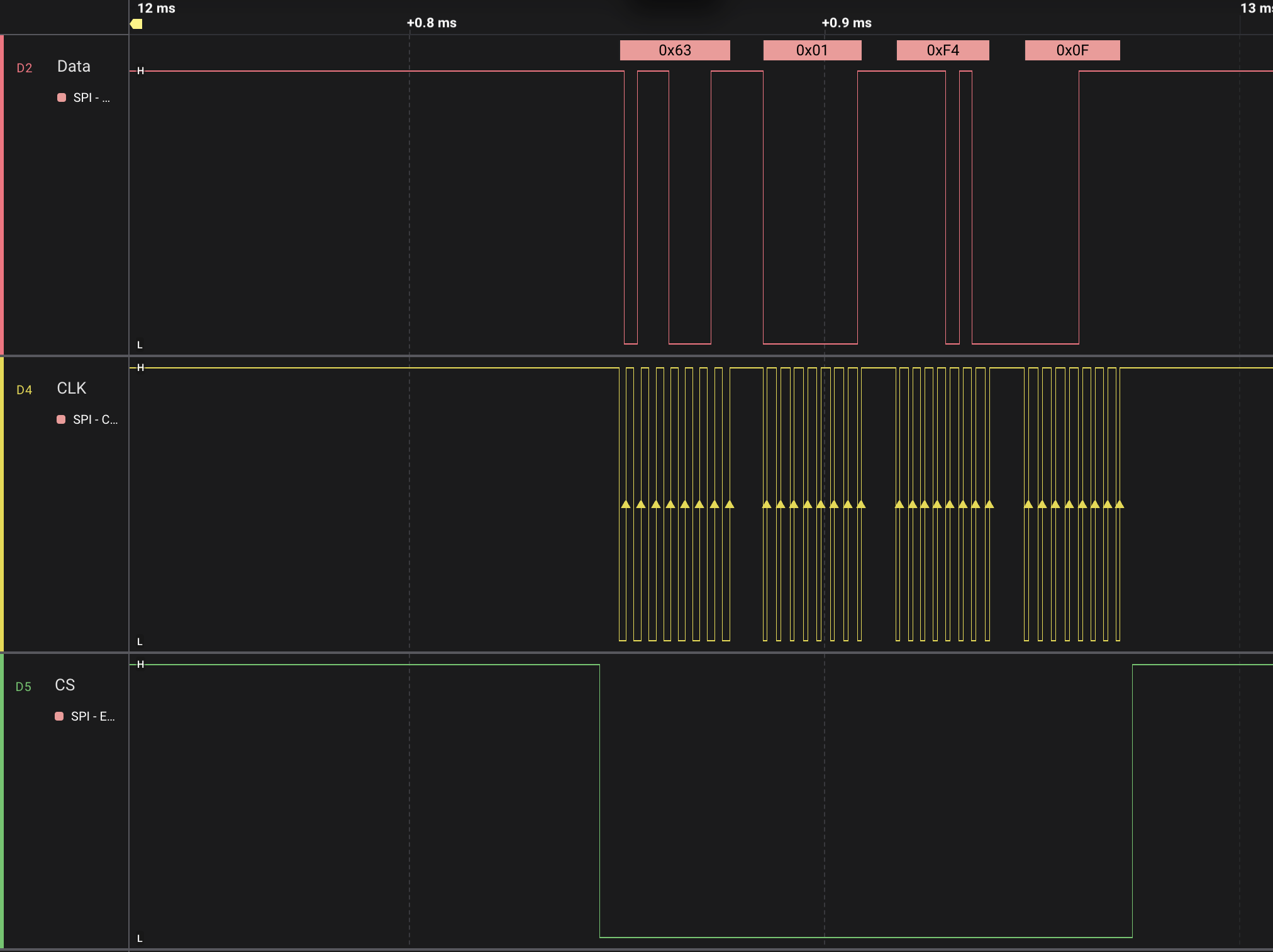
The first byte is a read from register 0x63, the BURST_MOTION register. This
means the next three bytes are the values of the DELTA_X, DELTA_Y, and
SQUAL registers.
The ADNS-3050 data sheet mentions that the data type for the DELTA registers
is eight bit 2’s compliment. This means the value of 0x01 is positive 1 in
the x direction and the value of 0xF4 is -12 in the y direction.
The ADNS-3050 data sheet says:
SQUAL (Surface Quality) is a measure of the number of valid features visible by the sensor in the current frame. The maximum SQUAL register value is 128
I’m a bit curious what the EX-G does with SQUAL. It seems like it should be
fairly constant since the sensor is looking at the trackball at a fixed
distance. Perhaps there is a low enough value where the EX-G ignores the
movements.
DPI Levels
I had captured the SPI messages used for changing DPI levels in the previous post. Repeating the values here for posterity.
| Mode | Command | Register | Value |
|---|---|---|---|
| 750 DPI | Write | 0x0D RESOLUTION | 0x83 |
| 1500 DPI | Write | 0x0D RESOLUTION | 0x86 |
Power Modes
High speed mode was captured by having the EX-G first powered on in low power
mode. With Logic Pro 2 set to capture the falling edge of CS and without
touching anything else on the EX-G, the switch was transitioned from low power
to high speed.
I was a bit surprised by this capture. I thought it was going to be changing one or two registers like the DPI change. It actually ran through a complete reset cycle similar to the power on cycle. There were some settings omitted though. The setting of registers 0x39 to 0x37 from the above power on list, were omitted.
It seems that the high speed mode resets everything and then omits setting the power down registers, as well as the frame rate and shutter registers.
The list of registers that high speed mode sets during the power on configuration phase:
| Command | Register | Value |
|---|---|---|
| Read | 0x00 PROD_ID | 0x3B |
| Write | 0x22 PERFORMANCE | 0x80 |
| Write | 0x1D UNKNOWN | 0x0A |
| Write | 0x14 UNKNOWN | 0x40 |
| Write | 0x18 UNKNOWN | 0x40 |
| Write | 0x34 UNKNOWN | 0x28 |
| Write | 0x64 UNKNOWN | 0x32 |
| Write | 0x65 UNKNOWN | 0x32 |
| Write | 0x66 UNKNOWN | 0x26 |
| Write | 0x67 UNKNOWN | 0x26 |
| Write | 0x21 UNKNOWN | 0x04 |
| Write | 0x22 PERFORMANCE | 0x00 |
| Write | 0x0D RESOLUTION | 0x86 |
| Read | 0x1A AXIS_CONTROL | 0x00 |
| Write | 0x1A AXIS_CONTROL | 0xA0 |
| Write | 0x42 BURST_READ_FIRST | 0x03 |
| Read | 0x02 MOTION | 0x00 |
| Read | 0x03 DELTA_X | 0x00 |
| Read | 0x04 DELTA_Y | 0x00 |
I will likely only implement the high speed behavior for my wired solution.
I seem to recall that some people were complaining about the EX-G battery life. I wonder if these people were leaving it in high speed mode and it was never going into the rest states.